Page 1 of 1
hbar beta, aka hbar's first adventure into Topre land
Posted: 08 Dec 2015, 13:48
by hbar
It is I, ħ, who has ventured with Arthur, King of the Britons, traveling far and enduring many hardships, in our quest to seek the Holy Grail of Input Devices. During our perilous journey from the crowded country of QWERTY, we were helped by many an African (or was it European?) swallow to the Castle of AAAAAAdNW, even encountering the knights who say "MX!" and defeating the Vintage Black Knight on the way. We seek the finest and greatest to join us on my Rectangular Table. The Holy M Hammer has proven to me that it is not required to cross the ALPS to reach the Topre, but also that xwhatsits will not be of any help, and that I shall count two, not one and not three, tiny bits when looking at my Rectangular Table.
In other words, split AdNW is great, but MX is still MX, so we need another shrubbery. Therefore, we shall let the Enchanter do his work.
ħ
Posted: 08 Dec 2015, 15:35
by hbar
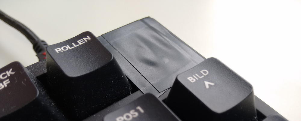
The first of many true believers in my cause that made a brave sacrifice was my current workhorse Sir Novatouch. It had to surrender the innards of one of its 88 limbs in order to further the advance in desktop technology we are all working hard to achieve:

- hb1.jpg (32.49 KiB) Viewed 7820 times
That valiant deed deserves true recognition.
ħ
Posted: 08 Dec 2015, 16:17
by andrewjoy
What foul deed did you enact upon the proud and noble novatouch ?
Posted: 08 Dec 2015, 17:43
by Stabilized
hbar wrote: ↑
That valiant deed deserves true recognition.
ħ
Tis but a scratch!
Posted: 08 Dec 2015, 20:27
by hbar
'Tis indeed!
Thou shalt blow your kitchen foil to tiny bits, ending up like this:

- hb2.JPG (50.6 KiB) Viewed 7760 times
The sacred Novatouch parts can be seen scattered all over the place.

- hb3.JPG (29.58 KiB) Viewed 7760 times
Measuring with a multimeter, the capacitance between the two half-moon-ish electrodes increases from essentially 0 to about 2pF when the key bottoms out.
ħ
Posted: 23 Jun 2016, 23:30
by hbar
After several months of going around in circles, it turned out that the fine test boards supplied by friendly Topre expert
workshop-f7/designing-a-custom-topre-board-t11734.html made all the difference in this development.
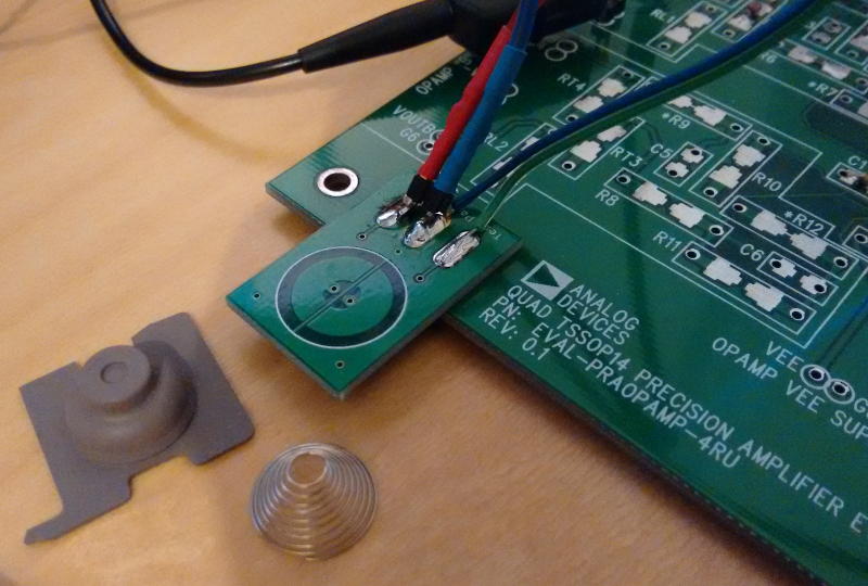
- board.jpg (69.38 KiB) Viewed 7596 times
The board now finally allows me to start debugging: it is solid, it can be kept in place, and it can be contacted with proper wires and proper solder joints. I now have my hands free and can start looking for the source of that horrible 50Hz interference (which the board didn't help with, unfortunately).
All I know so far is that the 50Hz is probably due to the haphazard wiring (inherent in a test circuit of this kind), but the circuit works in principle and the 50Hz is probably going to go away once I make a proper PCB with careful grounding.
ħ
Posted: 23 Jun 2016, 23:45
by hbar
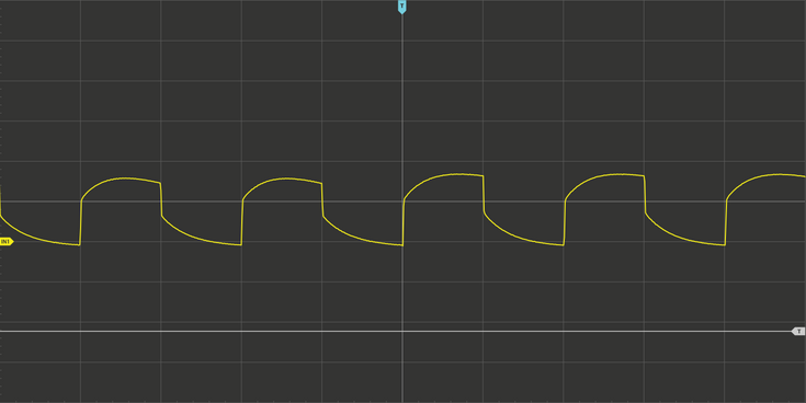
So here are the first results. This is the output voltage of the amplifier when the key bottoms out:
- on.png (25.87 KiB) Viewed 7589 times
The scale here is 500µs/div (pulse frequency is 1kHz), and 1V/div. This is with an excitation amplitude of just 1V, a standard CMOS circuit will produce at least twice as much, so the signal will also scale up accordingly. The fact that the shapes of the pulses differ slightly is that 50Hz interference that still needs to be dealt with.
This is with the key pressed only partially, probably close to the (very high) actuation point of the Novatouch:

- half.png (19.42 KiB) Viewed 7589 times
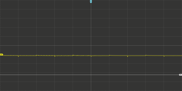
I made a mistake when trying to make a screenshot with the key released altogether, but the signal simply gets weaker, almost to the point that the pulses disappear. Measuring the voltage on the line from the switch to the amplifier results in this:
- error.png (18.96 KiB) Viewed 7589 times
This is on the same scale as the above, so the voltage on that line (and therefore any potential crosstalk) is negligible. The picture is almost completely independent of whether the key is pressed or not.
The beautiful thing is that this circuit is only a slightly modified transimpedance amplifier with a minimal parts count, but it still generates a very high-level signal compatible with any CMOS microcontroller ADC or comparator input while making the keys fully independent (no crosstalk). No analogue switch or digital resistor required, just one OP amplifier channel per detection line. Also, since we detect charge, not RC response (with its decay time), the slew rate of the driver is irrelevant and can be any CMOS logic output (microcontroller pin!) as long as the voltage swing is reproducible.
ħ
Posted: 24 Jun 2016, 08:46
by attheicearcade
Good to hear they help! What resistance is there between the row line and ground?
Posted: 24 Jun 2016, 09:04
by hbar
Resistance is essentially zero, it's a transimpedance amplifier after all. It's not quite zero because the OP amp is of limited speed, and there is trace resistance of course.
ħ
Posted: 24 Jun 2016, 09:48
by attheicearcade
Ah so it is a different method to mine. I found that my row line was just working as an antenna, picking up the mains signal from nearby power cables. Eliminated the majority of the noise by lowering the resistance to ground.
Posted: 24 Jun 2016, 10:00
by hbar
Yes, it's one of the reasons I picked the transimpedance approach. I'm quite certain that the 50Hz mains interference I struggle with comes from places other than the row lines because the transimpedance amplifier is sensitive to current, not voltage, so in order to influence the result significantly, the induced voltage on the row line would have to compete with the excitation signal (2-3V), which it certainly doesn't.
Contrary to your experience, my Novatouch didn't generate any voltage on the row lines that I could detect with my then-workhorse Fluke scope when I tested it last year, which made me think that Topre boards use a similar approach to mine, except they need a digitally controlled resistor and an analogue switch/multiplexer, which mine doesn't.
ħ
Posted: 24 Jun 2016, 11:05
by attheicearcade
Bear in mind that I tested the HHKB, not the Novatouch. The voltage pulses entering the TP1674 chip were very similar to the ones entering the op amp in my setup.
Posted: 27 Jun 2016, 19:39
by DMA
hbar, can you please explain to an uneducated person (i.e. me) how TIA works? Or at least point me to the good webpage about that.
I am _very_ interested in that "resistance is essentially zero" approach. It looks like it's what IBM does in those square white chips they use in their capacitive keyboards.
Posted: 28 Jun 2016, 11:23
by hbar
Here is an article that explains the general concept:
https://en.wikipedia.org/wiki/Transimpedance_amplifier
Mine has a few special details that are different, but I haven't got the time to go into that now (and no functioning schematic editor that I could use in hurry).
Posted: 28 Jun 2016, 16:53
by DMA
One would still need ADC or at least comparator to use that?
Posted: 28 Jun 2016, 23:03
by hbar
True, but modern microcontrollers come with both, and signal levels are, as you can see in the scope shots above, quite reasonable, so even a crappy 10 bit ADC would do the job.
Designing a PCB is next on my list, assuming for now that the 50Hz comes from the large loops in that proto board I used. Don't hold your breath for now, I've got so many other things to do (with much more severe physical retribution in case I don't deliver in time, not just harmless bumps of this thread).
ħ
Posted: 18 Jul 2016, 19:54
by hbar
I promised to myself that I wouldn't post to this thread until I have some more results. So I managed to keep my promise, since brand-new PCBs arrived today from China, and I couldn't but start soldering straight away. Just the controller module for now, which appears fine on the SWD debugger link connected through traces on the PCB, so that's a sign that the PCB isn't all rubbish:
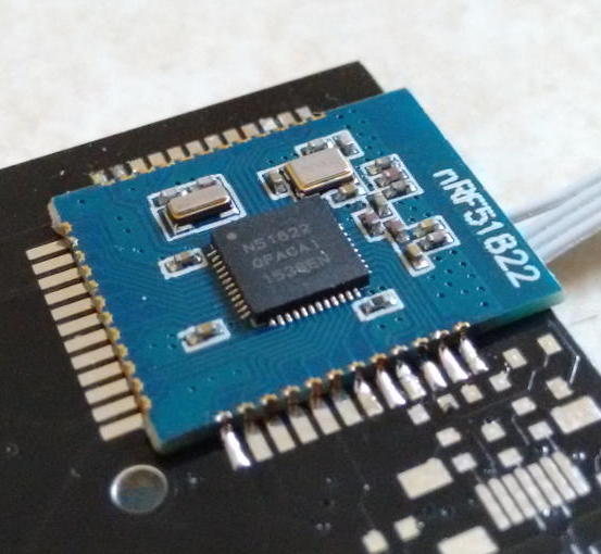
- 2.jpg (51.1 KiB) Viewed 7308 times
As it happens, this is the first PCB I ever sent off for manufacturing without printing the layout on paper first and test-placing the components, so every part I can solder without problems makes me happy.
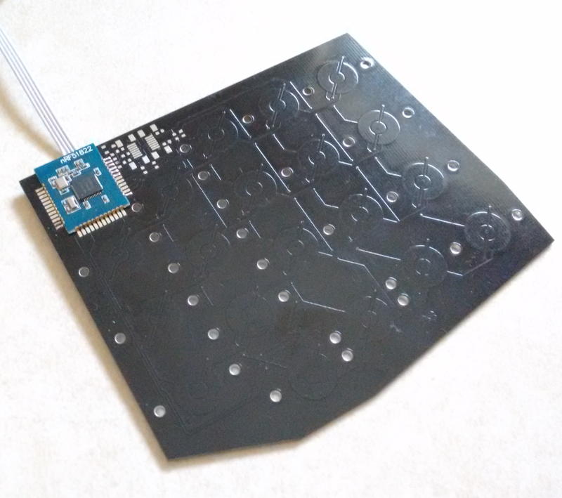
- 1.jpg (59.7 KiB) Viewed 7321 times
Sorry for the potatoes.
ħ
Posted: 18 Jul 2016, 21:58
by hbar
Oh joy, after a number of failures (with corresponding error messages from OpenOCD) and reading a lot of info on the net about how my Bus Blaster can't deal with the nRF51, the test code I wanted to flash miraculously appeared out of nowhere:

- s.png (14.36 KiB) Viewed 7294 times
Now let's move to some simpler GPIO logic. (The test was from Nordic's SDK, I haven't done any programming yet.)
Posted: 19 Jul 2016, 08:02
by DMA
What's the excitation impulse form? Square wave? Why current seems to be raising then - shouldn't it shoot to the max and then fall to zero in a log-like pattern?
Are you underdriving the line so hard it takes 250µs to peak excitation voltage?
Also I'm curious - can you overdrive the line with TIA on the sense end? Is it supposed to suppress ringing?
Posted: 19 Jul 2016, 13:13
by hbar
The excitation is a rectangle. Since the integrating TIA measures charge, you don't see the spikes typical of the RC circuits you and others (xwhatsit etc.) use. The limited skew rate is probably due to the extra resistor I installed for my tests in an attempt at combatting 50Hz interference. I'll post new graphs as soon as I have them. At the moment, I'm setting up a proper build environment for the nRF51822 so I can use it as the scan generator with the correct/final voltage swing etc.
ħ
Posted: 19 Jul 2016, 17:06
by DMA
hbar wrote: ↑The excitation is a rectangle. Since the integrating TIA measures charge, you don't see the spikes typical of the RC circuits you and others (xwhatsit etc.) use. The limited skew rate is probably due to the extra resistor I installed for my tests in an attempt at combatting 50Hz interference. I'll post new graphs as soon as I have them. At the moment, I'm setting up a proper build environment for the nRF51822 so I can use it as the scan generator with the correct/final voltage swing etc.
ħ
How does current to voltage converter measure charge? Wouldn't it just discharge capacitor via itself?
50Hz interference is easy to account for - have an exposed empty pad, it will collect the reference signal.
Posted: 20 Jul 2016, 16:14
by hbar
Let's see some pictures!
First of all, the set-up is quite a mess, as always:

- p.jpg (64.35 KiB) Viewed 7207 times
As you can see, I'm testing with a single key only, just to see whether it works at all.
Now the first results, for a single row. Key present but not pressed:
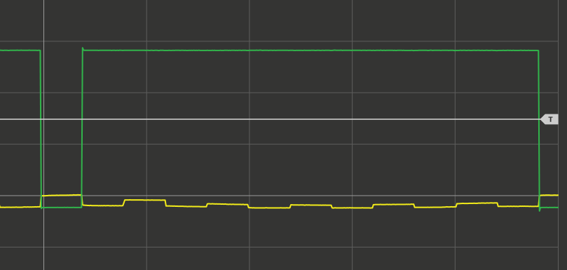
- 1c.png (11.2 KiB) Viewed 7207 times
Key partially pressed, around actuation point, you can clearly see some 50Hz as well there:

- 2c.png (12.25 KiB) Viewed 7207 times
Key fully pressed -- you can see the overall signal level rise somewhat, that's because the sense capacitor is too small, I'll have to try a larger one next time:

- 3c.png (12.83 KiB) Viewed 7207 times
All graphs are at 1V/div and 5ms/div. The green plot is the reference excitation output from the controller (an extra column with fixed capacitors instead of Topre electrodes) and allows me to trigger the scope on a scan frame. Timing is (sort of) arbitrary at the moment, I just used the timers already in the SDK example my code is based on.
The yellow plot is the output of one of the row amplifiers, which is also connected directly to an ADC input of the controller, with the goal of measuring the key states using that ADC, so this signal is what the ADC will eventually sample. By principle, there is an unpredictable offset of the entire curve (which we'll have to live with), but the plateaus before and after each rising edge are very nice and flat, so there is plenty of time for the ADC to sample them. The idea is, therefore, to read the column signals before and after each excitation pulse (which is a falling edge of the row drive signal, resulting in a sharp rise in ADC input signal) and compute the difference.
I can already hear Sir Novatouch scream "Run away, run away!!!". What a coward after all, I never would have expected to run into such resistance once I needed another bunch of his guts. Luckily enough, he stepped onto a coconut while sneaking away, which gave away his position and allow me to arrest him. He will be publically separated into his bits, that's the punishment he deserves.
ħ
Posted: 20 Jul 2016, 17:07
by DMA
How do you get those 2us steps on the input from the stable excitation level?
Posted: 21 Jul 2016, 00:09
by hbar
Since there is no resistor in the design, the rise time is only affected by the slew rate of the controller output and the bandwidth of the amplifier, which are both in the µs ballpark.
I quickly tried the board again with six switches haphazardly fixed with M2 bolts and nuts (thanks to Sir Novatouch being stripped of his valuable parts), and there were no surprises, but I didn't take any screenshots. Most importantly, there was no crosstalk to be observed between keys.
ħ
Posted: 21 Jul 2016, 02:20
by DMA
hbar wrote: ↑Since there is no resistor in the design, the rise time is only affected by the slew rate of the controller output and the bandwidth of the amplifier, which are both in the µs ballpark.
But wouldn't voltage on TIA output drop to zero once voltage stops rising? I mean, wouldn't measure window be very short?
hbar wrote: ↑
Most importantly, there was no crosstalk to be observed between keys.
Yes, that's just wonderful, other methods produce A LOT of crosstalk

Posted: 03 Aug 2016, 11:52
by hbar
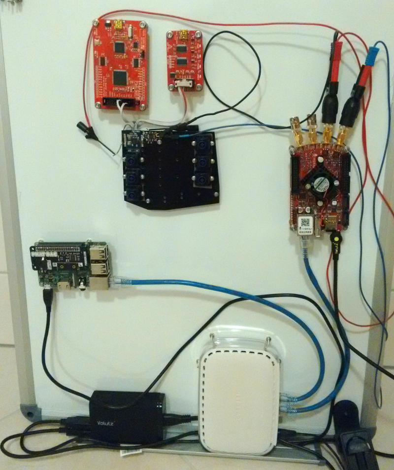
Finally sorted the electronics out:
- h.jpg (105.19 KiB) Viewed 7108 times
So as soon as I have some time, I can do some SPIS and ADC development work.
