KiCAD keyboard PCB design guide
| This article may require cleanup to meet Deskthority's quality standards. The specific problem is: This article was written for an old version of KiCAD, and should be updated for the current version Please improve this article if you can. The talk page may contain suggestions. |
Contents
KiCAD
KiCAD is an open source software for designing electronic schematics and transferring them to a PCB layout. All files it produces are text files which is quite straight forward to hack by hand or write custom scripts to handle. It is multi platform and available for Microsoft Windows and OS X as well as Linux. This guide will be focusing on Ubuntu Linux, and there are no guarantees of compatibility with other platforms.
Installing KiCAD
See the official KiCAD download page for installation instructions.
Eeschema
Eeschema is the schematics editor in KiCAD. Here components are defined and connected to form the schematics for your project.
Controls
Right clicking an object in the schematic brings up a list of edit options applicable to it. Most of these commands are also available as keyboard shortcuts. Hovering the mouse pointer over an object and pressing the corresponding key, the command is applied to it. Sometimes when there are several objects under the pointer a list of choices pops up. Stacking things to tightly can get annoying... Many of the shortcuts are also available when a component is picked up for moving. The shortcut is then applied to the floating object.
Keyboard shortcuts
This is only a selection of available commands.
m - Pick the component up for moving around.
g - Drag the component (move it while extending wires connected to it maintaining connectivity).
c - Copy the component.
e - Open the edit dialogue for the component, reference field or value field.
r - Rotate the component.
y - Mirror component.
Del - Delete the component
Esc - Abort a move (including orientation changes during the move).
It is also possible to select a block of items by drawing out a rectangle using the mouse. When a block is selected a left click brings up a list of applicable commands.
Creating a keyboard schematic
A keyboard matrix is really only a bunch of switches, each connected to a unique row-column pair to be able to tell them apart. To avoid ghosting this set-up is then improved by placing a diode in series with each switch.
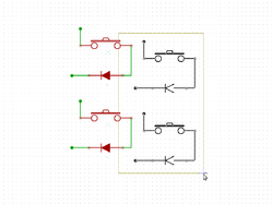
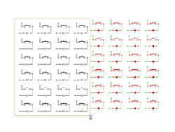
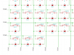
In KiCAD first drawing out a single switch-diode unit, making several copies to form a column, and then copying the columns into a complete matrix yields quick results. (Don't forget the junctions at the end of the leads.) Draw out a rectangle around the part you want to copy, right click and select Copy Block. Place components straight and tidy! Each iteration doubles the amount of new switches for an exponential growth. When all the switch modules are laid out they need to be connected to form rows and columns. There is no need to draw a wire segment between each pair of junctions, a long one overlapping them all is sufficient.
Each component also needs a unique reference. References can be almost anything, but they need to end in a digit. The quick and dirty way to assign references is to use the annotation tool in the top toolbar. This will assign a generic reference number to each component left-to-right/top-to-bottom. A more elegant way is to name the components after their spot in the key matrix. This needs to be done by hand (why not write a script!), but it will pay off in the end. Also add labels to the row and columns.
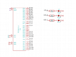
Next up is the controller. First off be sure to read and understand the 500+ page datasheet for the ATmega32u4... no, this is actually quite simple. Add labels for the rows and columns to the I/O-pins you would like to use. Any I/O-pins on the Teensy work equally well. You may want to swap pins around later to make routing a bit less tangled up. Add power symbols (VCC, GND), and also add some LEDs with current limiting resistors. Remember to set references for all of these components as well. Remove switches in locations you are not going to be using. And tidy up, always let your OCDs flourish.
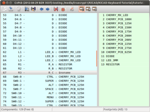
Now the schematic is done and all that is left is to create a netlist file, and assign footprints to each component. If all references are in order this is as simple as clicking the Generate netlist button in the top toolbar. When your netlist is generated, click the Run CvPCB button to assign the footprints. Assigning footprints to all components includes a lot of mouse clicking. This can of course be avoided by opening the tutorial.cmp file in an editor, apply some regular expression skill, and magically make component names appear in the correct places... Save the component assignment file, quit and open PCBnew from the KiCAD main window.
PCBnew
Pcbnew is the PCB editor in KiCAD. Here the modules (footprints) corresponding to your components are placed on the board, and traces are routed to connect them.
Keyboard shortcuts
m - Pick the footprint up for moving around.
g - Drag the footprint (move it while extending wires connected to it maintaining connectivity).
e - Open the edit dialogue for the footprint.
r - Rotate the footprint.
f - Flip the footprint (mirror and move between back/front).
Del - Delete the footprint.
Esc - Abort a move (including orientation changes during the move).
Space - Place the origin at the current mouse pointer location.
It is also possible to select a block of items by drawing out a rectangle using the mouse. When a block is selected a right click brings up a list of applicable commands. Esc aborts the move
Placing components footprints
Import all the components defined in the Eeschema schematic editor by clicking the Read netlist button in the top toolbar. This ends you up with all components nicely stacked on top of each other. Spend some time shuffling everything out to get some overview. The more keyboard oriented way of sorting out the mess is to use the shortcut t which let you pick up a component by specifying its reference. Next place some switch in a tactical integer coordinate location. Have the grid set to inches - keyboards are standardized in them, and the KiCAD internal representation is in inches anyway. Landing Esc on (0,0) can be a good idea for example. Continue placing all the switches correctly spaced. The c-c distance of two single unit wide keys should be 0.75". Setting the custom grid to 0.1875" is very helpful. The c-c distance between any two switches should be the average of their individual width, the distance between a 1.25u and a 6.25u key would be 0.75"x(1.25+6.25)/2. This quickly gets messy - make yourself a spreadsheet of all switch locations you intend to use. It would be great if the grid could be set to 0.75"/8=0.09375". Unfortunately this is below the preset 1/10000" tolerance. The bottom line of this is that you need to enter some of the switch locations by accessing the edit menu of the component, and enter the coordinates manually.
Mounting plates
The footprints contain mounting plate cutout shapes on the Eco2 layer. Shape objects need to be added to this layer for the plate outline, as well as any mounting holes needed. When this has been done the Eco2 layer can be exported as an Autodesk DXF file. This is a widely used CAD file format accepted by any respectable machine shop. Exporting is done under the "File->Plot" menu in Pcbnew.
Use setting:
- Plot format: DXF
- Layers: Eco2
- Plot mode: Line
The DXF files can be viewed with QCAD. Their community edition is open sourced.
External links
- KiCAD official homepage Retrieved 2024-04-09.
- Wikipedia on the AutoCAD DXF file format Retrieved 2024-04-09.
- QCAD official homepage Retrieved 2024-04-09.
- Tutorial example files Retrieved 2024-04-09.

